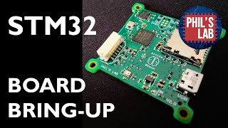
Sponsored
Sponsored
View Detailed Profile
(Sponsored) PCB Vias 101 - Phil's Lab #77

(Sponsored) PCB Vias 101 - Phil's Lab #77

Basics, guidelines, and best practices for

(Sponsored) PCB & Schematic Tip: Net Ties - Phil's Lab #69

(Sponsored) PCB & Schematic Tip: Net Ties - Phil's Lab #69

How to use net ties to increase schematic and

Sponsored
(Sponsored) How To Improve Your PCB Designs (Common Mistakes) - Phil's Lab #18

(Sponsored) How To Improve Your PCB Designs (Common Mistakes) - Phil's Lab #18

A look at common

77 Second Webinars: RF Via Fill

77 Second Webinars: RF Via Fill

RF

PCB Traces 101 - Phil's Lab #112

PCB Traces 101 - Phil's Lab #112

Basics and guidelines for

Sponsored
(Sponsored) ESD Protection Basics - TVS Diode Selection & Routing - Phil's Lab #75

(Sponsored) ESD Protection Basics - TVS Diode Selection & Routing - Phil's Lab #75

Basics of ESD protection in hardware and

(Sponsored) STM32 Board Bring-Up (Firmware and Test) - Phil's Lab #54

(Sponsored) STM32 Board Bring-Up (Firmware and Test) - Phil's Lab #54

Basic board firmware bring-up of the 'new' LittleBrain++
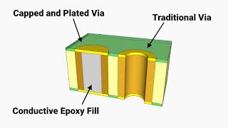
BGA PCB Design Tips - Phil's Lab #95

BGA PCB Design Tips - Phil's Lab #95

Incorporate ball-grid array (BGA) ICs into your

USB 3.1 to Gigabit Ethernet Adapter Hardware Design - Phil's Lab #174

USB 3.1 to Gigabit Ethernet Adapter Hardware Design - Phil's Lab #174

Schematic,

(Sponsored) How To Learn PCB Design (My Thoughts, Journey, and Resources) - Phil's Lab #87

(Sponsored) How To Learn PCB Design (My Thoughts, Journey, and Resources) - Phil's Lab #87

Recommendations on how to approach learning