Media Summary: In a previous video (link below), Tech Consultant Zach Peterson examined Multidisciplinary product creation powered by your unconstrained network. Work concurrently across design, sourcing, and ... In this video I will show you the basic principles behind

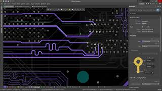
High Speed Routing On A Two Layer Board - Detailed Analysis & Overview

In a previous video (link below), Tech Consultant Zach Peterson examined Multidisciplinary product creation powered by your unconstrained network. Work concurrently across design, sourcing, and ... In this video I will show you the basic principles behind Recorded at AltiumLive 2019 Frankfurt. Pre-register for AltiumLive 2020: Recently we've gotten a few questions about Learn how to design a real computer with KiCad

Photo Gallery

High-Speed Routing on a Two-Layer Board
Can You Route USB 2.0 on a 2-Layer Board?
2-Layer PCB Design Tips - Phil's Lab #137
(Sponsored) High-Speed PCB Design Tips - Phil's Lab #25
How to Route High-Speed Designs in Altium Designer
Two-Layer PCB Design Tips: Achieving the Optimal Layout
High Speed PCB Design: How-To? Mastering The Basics For Success
High Speed PCB Design Tutorial | High Speed PCB Design Training Session - 1 | myTectra
Voltage Regulator Layout on a 2-Layer Board | PCB Routing Tips
Routing High Speed Boards in the 5G Era
What Are High-Speed PCBs? | Answering Your Questions!
EEVblog #1176 - 2 Layer vs 4 Layer PCB EMC TESTED!
Sponsored
Sponsored
View Detailed Profile
High-Speed Routing on a Two-Layer Board

High-Speed Routing on a Two-Layer Board

Two

Can You Route USB 2.0 on a 2-Layer Board?

Can You Route USB 2.0 on a 2-Layer Board?

In a previous video (link below), Tech Consultant Zach Peterson examined

Sponsored
2-Layer PCB Design Tips - Phil's Lab #137

2-Layer PCB Design Tips - Phil's Lab #137

Tips for designing with only

(Sponsored) High-Speed PCB Design Tips - Phil's Lab #25

(Sponsored) High-Speed PCB Design Tips - Phil's Lab #25

Quick overview of some general

How to Route High-Speed Designs in Altium Designer

How to Route High-Speed Designs in Altium Designer

Multidisciplinary product creation powered by your unconstrained network. Work concurrently across design, sourcing, and ...

Sponsored
Two-Layer PCB Design Tips: Achieving the Optimal Layout

Two-Layer PCB Design Tips: Achieving the Optimal Layout

Multidisciplinary product creation powered by your unconstrained network. Work concurrently across design, sourcing, and ...

High Speed PCB Design: How-To? Mastering The Basics For Success

High Speed PCB Design: How-To? Mastering The Basics For Success

In this video I will show you the basic principles behind

High Speed PCB Design Tutorial | High Speed PCB Design Training Session - 1 | myTectra

High Speed PCB Design Tutorial | High Speed PCB Design Training Session - 1 | myTectra

Master the essentials of

Voltage Regulator Layout on a 2-Layer Board | PCB Routing Tips

Voltage Regulator Layout on a 2-Layer Board | PCB Routing Tips

Multidisciplinary product creation powered by your unconstrained network. Work concurrently across design, sourcing, and ...

Routing High Speed Boards in the 5G Era

Routing High Speed Boards in the 5G Era

Recorded at AltiumLive 2019 Frankfurt. Pre-register for AltiumLive 2020: https://www.altium.com/live-conference/registration.

What Are High-Speed PCBs? | Answering Your Questions!

What Are High-Speed PCBs? | Answering Your Questions!

Recently we've gotten a few questions about

EEVblog #1176 - 2 Layer vs 4 Layer PCB EMC TESTED!

EEVblog #1176 - 2 Layer vs 4 Layer PCB EMC TESTED!

What difference does a 4

High-Speed PCB Design Guidelines – Understanding Signal Integrity and Impedance in KiCad

High-Speed PCB Design Guidelines – Understanding Signal Integrity and Impedance in KiCad

Learn how to design a real computer with KiCad